Cheaper production of an unsung industrial substance could make hard stuff a lot easier
Boron nitride has a tough reputation.
In its cubic crystal structure, cubic boron nitride, or c-BN, is one of the most remarkably-durable human-made materials ever invented, almost on par with natural and synthetic diamonds. It is widely used across aerospace, defense, energy, transportation, and other industries, in settings where products are intended to withstand truly extreme conditions, or when heavy industry needs to drill, cut, or ground such parts into shape.
The hardy stuff even holds up in highly reactive environments; it demonstrates superior stability against oxidation and unintended chemical reactions with, for example, iron, even at incredibly high temperatures.
Boron nitride also happens to be a semiconductor with electrical properties that could enable electronics manufacturers to build equipment that provide 3-4% greater power conversion efficiency than traditional, silicon-based technologies. Think about that: if you multiply that increase in efficiency by the number of electronic devices that require power conversion (hint–all of them), the positive economic and energy-consumption impact is staggering.
But, according to Siddha Pimputkar, an assistant professor of materials science and engineering at Lehigh University, the process of producing cubic boron nitride presents a significant obstacle, and boasts a reputation for being equally as stubborn as the material itself.
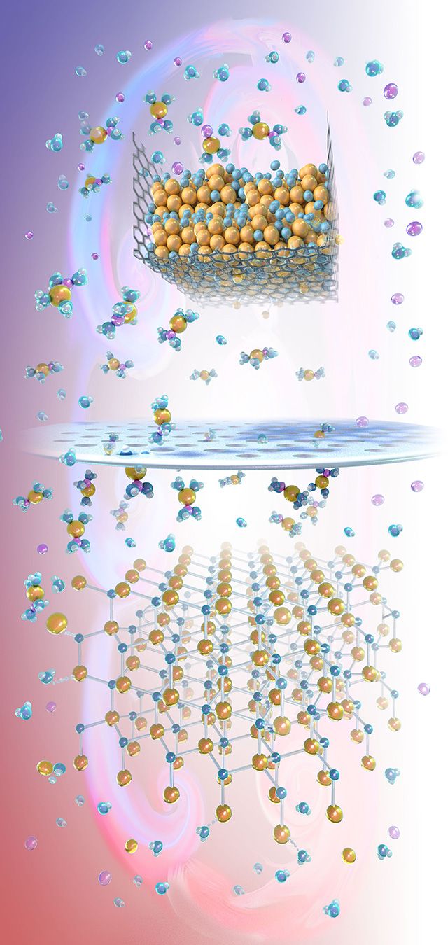
"Currently, the synthesis of cubic boron nitride is performed under high-pressure, high-temperature conditions, in the presence of suitable catalysts such as lithium or barium nitride," he says. "Under these constraints, synthesis is effectively unscalable, and the process of producing any amount of this material turns out to be enormously expensive and energy intensive."
Working with Kai Landskron, a professor of chemistry with Lehigh's College of Arts and Sciences, Pimputkar has recently won support from the National Science Foundation (NSF) to find a cheaper, greener way of producing boron nitride. The project, which formally kicked off on September 1, 2018, brings more than $450,000 in research support to the interdisciplinary Lehigh faculty team, both of whom are affiliated with Lehigh's Institute for Functional Materials and Devices. The funding will support their efforts to grow single, centimeter-sized crystals of boron nitride in conditions that are much closer to room temperature and pressure, using conventional, readily scalable autoclave systems.
Materials development, without all the drama
Pimputkar explains that boron nitride's true advantage compared to diamond lies in its ability to withstand high temperature while remaining chemically inert and operational—but current methods of producing it leave much to be desired.
"Synthesis of c-BN crystals is currently possible through the use of what are known as high-pressure anvil systems. It is quite an expensive proposition, and the size of the crystals produced is limited to somewhere in the range of a millimeter in diameter, which then limits the crystal's utility," he says. "Boron nitride has also been produced using a process known as chemical vapor deposition, or CVD. Yet this has not proven to be an economical method of bulk production either, and it yields smaller crystals as well."
Landskron says that the project seeks to synthesize much larger crystals of cubic boron nitride at a far lower cost and reduced energy consumption than ever before possible, and that this could open up new avenues of research and development in electronics.
"Development of c-BN single-crystal wafers would create a significant impact in the electronics community as novel, more efficient devices and applications become possible. This would lead to drastic reduction in power losses for high-voltage power electronics, as compared to the silicon technology in use today."
Pimputkar also believes that the project could have even broader implications through impact upon the field of high-pressure materials synthesis more generally.
"The practical value of materials synthesized at high pressure is currently quite limited," he says. "In order to drive wide-scale adoption, the process is simply not viable, and is not easily scalable to the levels that industry would typically need it to be. The techniques we are developing may prove to be applicable in the production of an array of other industrially-relevant materials, such as cubic silicon nitride."
According to the team, if the project is successful, it may also influence the future development of a wide array of technologies. Pimputkar says that other possibilities include efficient solid-state UV LEDs, lasers for use in disinfecting water, surfaces, and air, neutron detection, replacing the increasingly scarce He3 sources, and improved technologies for fundamental and planetary scientific research.
About the team
Siddha Pimputkar received his Ph.D. in Materials at the University of California, Santa Barbara (UCSB) working with Nobel Laureate Prof. Shuji Nakamura and Prof. Jim Speck. He now pursues research focused on enabling and developing advanced materials for use in novel electronic and optoelectronic devices. Focus areas in his Materials for Advanced Technologies and Sustainability (MATS) Lab at Lehigh include growth of single crystal III-Nitride materials (such as bulk GaN or AlGaN) or growth of thin films using novel equipment (High Pressure Spatial CVD) developed to enable growth of typically decomposition limited materials, such as high indium content III-Nitrides or oxynitrides. Pimputkar is developing improved methods of creating nitride crystals at scale that meet the demands for size and quality. Applications of novel materials developed in his lab will ultimately culminate in demonstrating, for example, energy efficiency power electronics or high efficiency UV emitters.
Kai Landskron received his diploma in Chemistry from University of Bayreuth, Germany in 1998. He received his Ph.D. in Chemistry from University of Munich (LMU), Germany working with Wolfgang Schnick on the synthesis of phosphorus (V)-nitrides. Following postdoctoral work in the research group of Geoffrey Ozin at University of Toronto, he joined the faculty of Lehigh University in 2006. His research encompasses synthetic high-pressure chemistry of porous materials, the synthesis of high-pressure phases near ambient pressure and temperature conditions, as well as gas separations using capacitive methods.