Innovations in material science are as essential to modern life as indoor plumbing―and go about as unnoticed.
For example, innovations in semiconducting devices continue to enable the transmission of more information, faster and through smaller hardware―such as through a device that fits in the palms of our hands.
Improvements in imaging techniques have made it possible to collect mounds of data about the properties of the nanomaterials used in such devices. (One nanometer is one billionth of a meter. For scale, a strand of human hair is between 50,000 and 100,000 nanometers thick.)
“The challenge is that analytical approaches that produce human-interpretable data remains ill-equipped for the complexity and magnitude of the data,” says Joshua Agar, an assistant professor of materials science and engineering. “Only an infinitesimally small fraction of the data collected is translated into knowledge.”
Agar studies nanoscale ferroelectrics, which are materials that exhibit spontaneous electric polarization―as a result of small shifts in charged atoms―that can be reversed by the application of an external electric field. Despite promising applications in next-generation low-power information storage/computation, energy efficiency via harvesting waste energy, environmentally friendly solid-state cooling and much more, a number of issues still need to be solved for ferroelectrics to reach their full potential.
Agar uses a multimodal hyperspectral imaging technique—available through the user program at the Center for Nanophase Materials Sciences at Oak Ridge National Laboratory—called band-excitation piezoresponse force microscopy, which measures the mechanical properties of the materials as they respond to electrical stimuli. These so-called in situ characterization techniques allow for the direct observation of nanoscale processes in action.
“Our experiments involve touching the material with a cantilever and measuring the material’s properties as we drive it with an electrical field,” says Agar. “Essentially, we go to every single pixel and measure the response of a very small region of the material as we drive it through transformations.”
The technique yields vast amounts of information about how the material is responding and the kinds of processes that are happening as it transitions between different states, explains Agar.
“You get this map for every pixel with many spectra and different responses,” says Agar. “All this information comes out at once with this technique. The problem is how do you actually figure out what’s going on because the data is not clean―it’s noisy.”
Agar and his colleagues have developed an artificial intelligence (AI) technique that uses deep neural networks to learn from the massive amounts of data generated by their experiments and extract useful information. Applying this method, he and his team have identified―and visualized for the first time―geometrically driven differences in ferroelectric domain switching.
A schematic drawing showing a 3-D rendering of a cantilever in contact with the surface of a ferroelectric material. Diagram shows how neural networks can be used to visualize spatial differences that can be correlated to the response mechanisms.
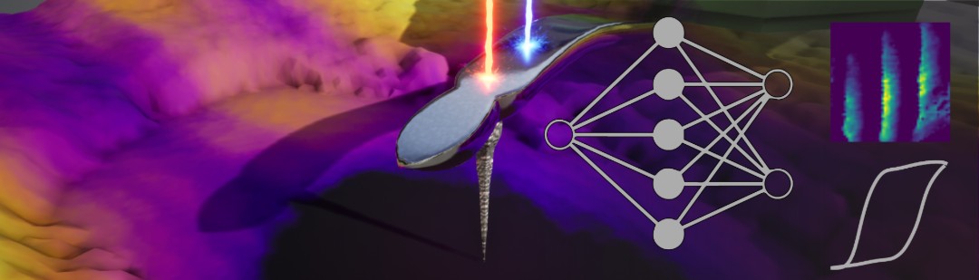
Image credit: Joshua C. Agar and Joshua Willey
The technique, and how it was utilized to make this discovery, has been described in an article published in Nature Communications called “Revealing Ferroelectric Switching Character Using Deep Recurrent Neural Networks.” Additional authors include researchers from University of California, Berkeley; Lawrence Berkeley National Laboratory; the University of Texas at Arlington; Pennsylvania State University, University Park; and the Center for Nanophase Materials Science at Oak Ridge National Laboratory.
The team is among the first in the materials science field to publish the paper via open-source software designed to enable interactive computing. Both the paper and the code are available as a Jupyter Notebook, which runs on Google Collaboratory, a free cloud computing service. Any researcher can access the paper and the code, test out the method, modify parameters and even try it on their own data. Agar hopes that by sharing data, analysis codes and descriptions, this approach will be used in communities outside of those who use this hyperspectral characterization technique at the Center for Nanophase Materials.
According to Agar, who is affiliated with Lehigh's three Interdisciplinary Research Institutes (IRIs) the neural network approach could have broad applications: “It could be used in electron microscopy, in scanning tunneling microscopy and even in aerial photography,” he says. “It crosses boundaries.”
Read the full story in the Lehigh University News Center.
Story by Lori Friedman