When you plug in your laptop, you might notice that the “brick” on the cable becomes warm to the touch. The generated heat is a sign that the charger is working, but it also represents energy losses.
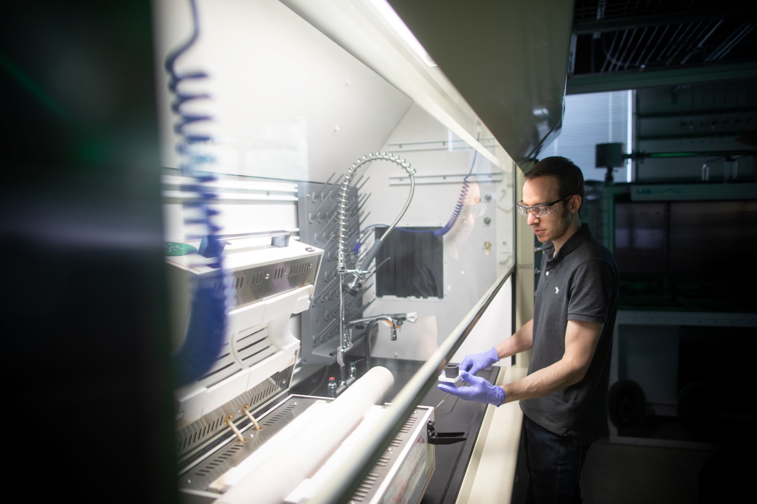
“If you take the silicon out of the transformer and put gallium nitride in, the transformer could be so much smaller and have almost zero energy loss,” says Florian Metzger (pictured above), a PhD student in materials science and engineering. “A laptop charger is small scale, but if you think bigger, power plants or transformer stations could become largely loss free.”
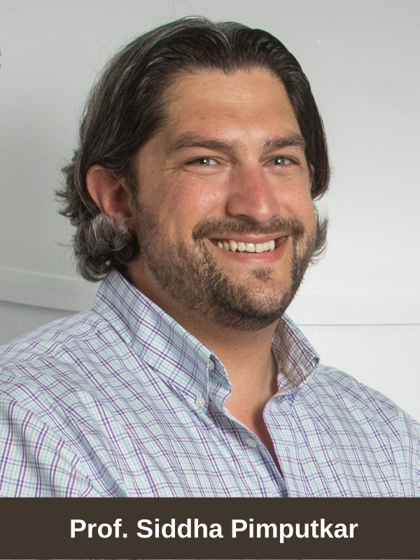 Metzger is a fifth-year doctoral student in Lehigh’s MATS (Materials for Advanced Technology & Sustainability) Group, which is led by Siddha Pimputkar, an assistant professor of materials science and engineering. Pimputkar and his team are focused on synthesizing bulk single-crystal, nitrogen-containing materials, including gallium nitride (GaN). The materials offer properties more “extreme” than those found with commonly used silicon, meaning they allow for more efficient energy transformation.
Because of current cost and crystal-size limitations of gallium nitride, the material is typically grown on sapphire wafers for use in semiconductor devices. Metzger’s research will explore a new method of producing synthetic GaN boules, or large single crystals, which can be thinly sliced to create wafers. In the future, the material could succeed silicon as the preferred energy-efficient material choice for use in electronic devices.
To grow GaN boules, Metzger is exploring an approach resembling one used to grow silicon boules. (The “Czochralski process” involves melting silicon in a crucible and slowly drawing it upward with carefully monitored variables; it has allowed perfect single-crystal silicon wafers to be produced over 1.5 feet in diameter at extremely low cost.)
“We hope we can make large wafers faster using this new approach, because we can then tap into all the exciting technologies already conceived, though not viable outside of a research lab due to limitations in GaN availability.” says Metzger.
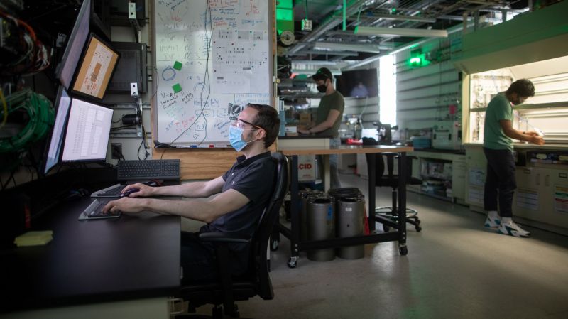
To achieve such a breakthrough requires developing equipment “outside the realm of what people use today,” says Pimputkar. The MATS team expects to have their cutting-edge research lab, which has been under construction for the past five years, fully functional in early 2022.
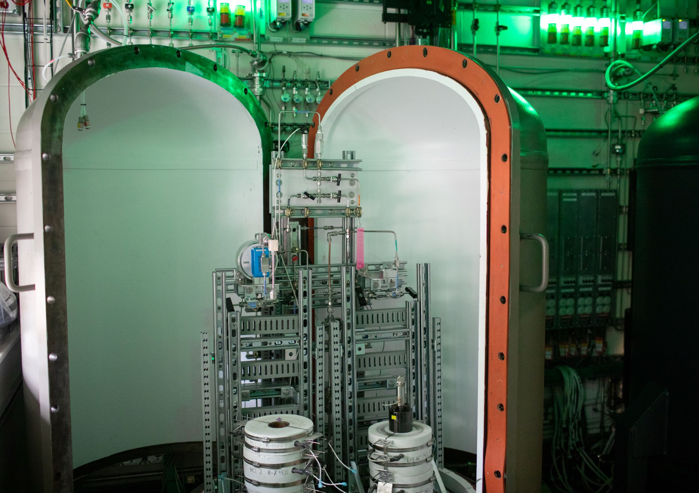
“Everything in the lab beyond the fume hoods and other typical infrastructure has been custom built to my specifications and design,” says Pimputkar. This includes the unique autoclave vessels in which the gallium nitride will be synthesized under extreme conditions.
“Developing our own equipment allows us to explore growth chemistries and conditions that others cannot,” he says. “We can radically change how we grow these crystals, significantly improve upon material quality or associated cost, or even walk into the unknown and discover new materials with exciting properties.”
The novel technologies incorporated into the lab’s growth equipment set it apart as a one-of-a-kind facility in the United States, says Pimputkar, if not the world.
Building the autoclaves has been an adventure, Metzger says. He compares them to pressure cookers, “but instead of operating at 2 atmosphere and 120° Celsius or so, we are operating at 100 atmospheres and 1000° Celsius using rather corrosive chemistries.”
 Once the autoclaves are fully operational, research will continue by refining the growth conditions and chemical composition of the system to yield GaN crystals. After mastering the production of the single crystals, Metzger will explore their properties and provide simple demonstrations of their utility for high-efficiency, high-power electrical energy conversion applications.
He expects many more technical challenges to arise, as is common for this type of experimentation, but he is optimistic about taking them on as part of the research process. He is excited to see the lab’s construction completed, allowing him to begin the materials research he came to Lehigh to do.
Metzger met Pimputkar at the University of California, Santa Barbara, in summer of 2016 while both were studying nitride synthesis. Pimputkar was a postdoc in the lab of Nobel laureate Dr. Shuji Nakamura (inventor of blue LEDs); Metzger was a master’s student in chemistry and biology engineering at FAU Erlangen-Nürnberg in Germany attending a summer school collaboration between the universities. Pimputkar became a member of the Lehigh faculty in August 2016, and Metzger joined his research group as a doctoral student the following year.
After Metzger completes his PhD, he plans to continue working on nitride synthesis, though his next steps are still to be determined.
“Maybe I’ll stay a little longer [at Lehigh] for a postdoc and do the research,” he says. “I put so much time and effort in building all this, but so far it’s just proof of concept.”
Metzger hopes more students will join the MATS lab to continue experiments on other nitrides, including boron nitride (BN), that have the potential to enable truly extreme devices and applications.
There are also materials (such as indium nitride, or InN) to explore that could enable high-efficiency optical emitters across the complete visible spectrum, says Pimputkar. Another research direction, he adds, is looking into materials composed of abundantly available elements that have properties ideal for use as functional materials, including semiconductors, by transitioning from pure nitrides to multi-anionic materials, including oxy-nitrides and carbo-nitrides.
As for long-term goals for his lab, Pimputkar aspires to develop the capabilities to grow a wide range of nitride materials “on demand” by using artificial intelligence (AI)-controlled growth systems designed by the MATS team in conjunction with existing material property/thermodynamic/kinetic databases.
“Numerous opportunities exist to enable a more sustainable future by either significantly improving the efficiency of current devices or enabling new devices using earth-abundant or sustainable elements,” says Pimputkar. “We think we will be able to synthesize these emerging materials in a way that is industrially scalable,” he says, “so it can eventually be translated to important advances in society.”
Story by Michelle Rodriguez ’21
Photography by Douglas Benedict/Academic Image