Half a century ago, the Nobel Prize-winning physicist Richard Feynman helped launch the era of nanotechnology when he told scientists to dream little, not big.
In an address to the American Physical Society, titled “There’s Plenty of Room at the Bottom,” Feynman told his audience they could develop tools capable of manipulating individual atoms and molecules.
Imagine putting a 24-volume encyclopedia on the head of a pin, Feynman said. Imagine 24 million books. Similarly scaled down, they could fit on 35 pages. What about computers? In 1959, they filled entire rooms. Why couldn’t they be made of wires just tens of atoms in diameter and circuits only a few hundred nanometers across?
Feynman did not talk of nanotechnology. A Japanese engineer, Norio Taniguchi, coined the term in 1974, and an American engineer, Eric Drexler, popularized it in 1986 with his book Engines of Creation: The Coming Era of Nanotechnology.
Fifty years after Feynman’s presentation, much of what he predicted has come to pass. Indeed, says Marvin White, consumers now demand a steady stream of miracle products with sizes – and price tags – locked in a never-ending downward spiral.
“Nano accounts for many major electronic advances of the past 10 years – cell phones, iPods, digital cameras, laptops, you name it,” says White, a member of the National Academy of Engineering and director of Lehigh’s Sherman Fairchild Center for Solid-State Studies.
“And there are applications of nano in almost every other field. Take waterproof clothing. Water runs off it because of nanoparticles embedded in the fabric. Look at health care. The response of cells to outside stimuli can be measured, and cell properties characterized, using nano research instruments.”
Nanotechnology has been defined as the engineering of systems with dimensions smaller than 100 nanometers. One nanometer (1 nm) equals one billionth of a meter or, as one wag put it, the length a man’s beard grows as he lifts his razor to his face.
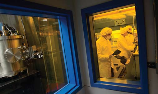
White is one of more than 50 Lehigh faculty members involved in nano research. These engineers, physicists, chemists and biologists collaborate in a variety of groups and venues, including the Center for Advanced Materials and Nanotechnology (CAMN), which is well-equipped for nanocharacterization, and the Center for Optical Technologies (COT) and Sherman Fairchild Center, which have expertise in nanosynthesis and nanofabrication.
Lehigh’s nano researchers have scored successes in sensors and transducers, catalysts and sorbents, photovoltaics and light sources, nanoparticles and quantum-dot synthesis, and high-density information management. These are impacting energy, environment, infrastructure and other areas. Palladium-coated iron nanoparticles developed at Lehigh, for example, are treating contaminated groundwater in half a dozen states.
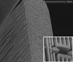
Lehigh’s bioengineering researchers also work at the nano level. Electrical engineers pursue nanophotonic biosensing on a chip. Physicists model the dynamics of the cell’s cytoskeleton. Materials scientists and mechanical engineers fabricate injection-molded nanostructures on which adult stem cells grow and differentiate (see p. 18).
An emphasis on the superficial
The key to nanotechnology research, says CAMN director Martin Harmer, is much what Richard Feynman envisioned – the control of molecules and atoms at the surfaces and interfaces that are a material’s most reactive regions.
“Our goal,” says Harmer, “is to equip surfaces and interfaces with desirable and predictable characteristics at the nanoscale. These include chemical composition and atomic structure, and structural, optical, conductive and magnetic properties.”
To understand the nano world, one must first observe it. Here, Lehigh offers an advantage: Its surface analysis and microscopy tools are among the world’s best.
“Each apparatus we have integrates a number of analytical methods,” says Bruce Koel, vice president and associate provost for research and graduate studies. “This gives us a tremendously powerful, multitechnique approach to complicated problems.”
Lehigh’s scanning probe microscopes, both scanning tunneling (STM) and atomic force (AFM), characterize surface topography in every kind of medium. The university’s Scienta ESCA 300, one of 11 in the world and the only one in the U.S., is one of the best x-ray photoelectron spectroscopy (XPS) instruments available for chemical analysis. The high-sensitivity, low-energy ion-scattering spectrometer (HS-LEIS), under acquisition through a 2008 NSF grant, affords unprecedented surface analysis and will be the first instrument of its kind in an academic lab.
“The Scienta enables us to study surfaces with a high sensitivity and resolution for chemical analysis,” says Koel, a professor of chemistry. “It gives us information about the near surface – the chemical composition of the top 10 atomic layers of a material. If you see aluminum, HS-LEIS tells you whether it’s metal or oxide. If you see carbon, HS-LEIS tells you whether it is bound to oxygen or to another carbon.
“But the very top or outer layer, which measures just 0.2 to 0.3 nm in thickness, is critical for chemical behaviors. HS-LEIS uniquely tells us what the topmost layer of atoms is.”
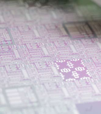
The electron microscopy facilities at Lehigh are comparable to those of a national lab. The university’s annual Microscopy School draws researchers from major government, industry and academic labs around the world. Lehigh was the first university to acquire two aberration-corrected transmission electron microscopes, which determine the chemical identity of atoms in crystals with a focused beam of 0.1 nm.
Materials scientists in the CAMN have developed software (see p. 5) that more efficiently analyzes data gathered from electron microscopes, improves signal-to-noise ratio, and achieves greater resolution of small concentrations of elements. Scientists also use a technique called High-Angle Annular Dark Field imaging to enhance resolution of crystal materials.
“This technique makes it possible to see individual metal atoms or atom clusters dispersed over oxides,” says Christopher Kiely, director of the CAMN’s Nanocharacterization Laboratory. “It turns out that these clusters or atoms often play a critical role in material behaviors.” (See p. 4.)
“The enhanced resolution of the aberration-corrected microscopes enables us to see what atoms really do,” says Harmer. “Coupled with our improved computational simulation of nanostructure devices, these microscopes have shown us that the scientific assumptions on which our knowledge rests are fragmentary or even fictitious. This leads to completely new thinking about interfaces.”
Nonvolatile memory
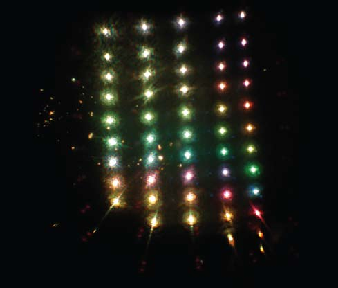
To design and fabricate electronic equipment, says Marvin White, one must first understand how electrons and holes move through nanostructures. The control of these charge carriers and their transport phenomena is vital to the nonvolatile storage of data, in which information is preserved without the use of an active power supply.
White has spent 40 years investigating nonvolatile semiconductor memory – the memory inside a thumb drive or an iPod, for example, which relies on the storage of electrostatic charge in the form of negative charge (electrons) and positive charge (holes).
“We model and study the transport phenomena of charge carriers both along the surface, covered by nanolayers of thin films, and perpendicular to this surface,” says White. “The carriers move along the surface in devices that switch and amplify information. In devices that store information, they move perpendicular to the surfaces by a process called ‘tunneling’ and are trapped in these thin films.
“We make our own devices, and we model the transport phenomena observed or created by other researchers. Our partners include Intel, Micron Semiconductor, IBM, AMD and Northrop Grumman.”
The phenomena that White and his students study often occur at what he calls the realm of the sub-nano, with features a few nm or smaller.
“The structures that switch, amplify and store information have dimensions on the order of 10 or 20 angstroms or less. One structure, a silicon-dioxide film grown with atomic layer deposition, is just 4 angstroms thick.” An angstrom is 0.1 nm.
Advanced tools, says White, are critical to his research. Electron beam lithography enables his group to create and investigate the properties of nonvolatile memory and scaled semiconductor devices. Angle-resolved photoelectron spectroscopy (ARXPS) helps determine a structure’s thickness by locating and identifying atoms at or near its surface. Fabricating these nanostructures requires integrating more than 100 process steps in the lab.
Conceptual changes
Nanotechnology research, says Martin Harmer, can reorder the familiar landscape of scientific knowledge. “We have recently discovered that interfaces are not accurately described as two-dimensional,” says Harmer, a professor of materials science and engineering. “The traditional idea was that an interface was a region of misfit between two well-defined crystals. The new idea is that an interface is a third region with its own identity and criteria for stability. It is in fact a new state of matter, neither amorphous nor crystalline, at the interface between crystalline grains.
“We did not appreciate that internal interfaces would behave in this fashion until we acquired the tools to examine them, namely, aberration-corrected microscopy.”
Harmer has coined the term “complexions” to describe these interfaces. He received the Robert B. Sosman Award from the American Ceramic Society in 2008 in part due to this fundamental discovery.
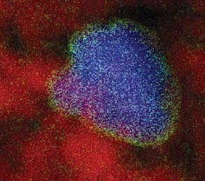
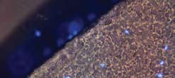
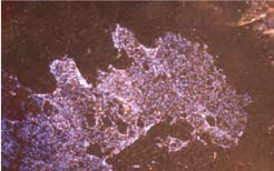
In another project, Harmer and Kiely have been synthesizing nanoparticles of iron oxide that enhance contrasts in an MRI, and characterizing the particles with TEM. Harmer and Kiely and their collaborators, who include physicists, chemists, mechanical engineers and biomedical researchers, hope to use the particles to improve the diagnosis and targeted treatment of breast cancer. The team, led by Winston Soboyejo of Princeton, includes researchers from Duke and Louisiana State Universities, as well as Makerere University in Uganda and Cheikh Anta Diop University in Senegal.
When knowledge precedes understanding
The nano world has always been with us, says Bruce Koel. What is new is our attempt to understand and control it to make new materials and devices.
“For example, people who work in catalysis pass crude oil over catalysts to get gasoline,” says Koel. “These catalysts have always been nanoparticles. What we are now trying to do is control their size, shape and features. To us, 2 nm is very different from 4 nm and a cube is very different from a sphere. This level of control is unprecedented.”
Koel’s point is illustrated by Israel Wachs, a professor of chemical engineering and noted catalysis expert. Wachs has learned that tungsten oxide, an acid used to boost octane in gasoline, is 100 times more reactive when attached to titania nanoparticles measuring 1 nm than when attached to titania measuring roughly 5 nm.
Himanshu Jain, professor of materials science and engineering, says “ruby glass” is another example of knowledge preceding understanding. Two millennia ago, without understanding why it happened, the Romans knew that gold dispersed in glass could cause the glass to take on a reddish hue. Not until the 1920s did scientists learn that colloidal nanoparticles of gold were responsible for imparting the red hue.
Jain has assembled an international team of researchers to explore the electrical properties of gold and silver nanoparticles distributed homogeneously in glass.
“The optical properties of gold nanoparticles distributed in glass are reasonably well-understood,” says Jain, who directs Lehigh’s NSF-supported International Materials Institute for New Functionalities in Glass, “but there is no literature on the electrical behavior of the nanocomposite material. Our theory is that we might see nonlinear electric properties and switching.”
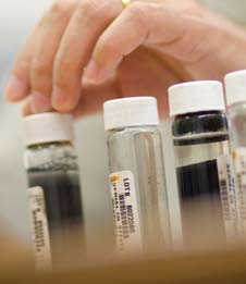
Jain and his team hope that particles of silver measuring 8 to 10 nm might facilitate the development of antibacterial glass. They are using the Scienta ESCA 300 to examine the chemical structure of the nanoparticles as they disperse in phosphate glass.
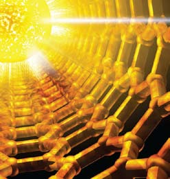
Silicon photonics
The silicon chip, says Tom Koch, an NAE member and director of Lehigh’s COT, combines economy of scale, precision and sophistication like no other technology. Its 1 billion transistors contain features as small as 45 nm, a size engineers hope to cut in half.
Koch wants to overcome silicon’s optical deficiency by exploiting its superior electronic properties and the precision with which it can be fabricated.
“As a manufacturing enterprise,” says Koch, a professor of both electrical engineering and physics, “nothing in history comes even remotely close to the chip.”
But silicon does not emit or detect lightwaves usable in most telecommunication applications, a shortcoming that would seem to rule out a central role in meeting the escalating demands for speed, size and power in next-generation networks.
Koch, working in an area called silicon photonics, wants to overcome silicon’s optical deficiency by exploiting its superior electronic properties. Researchers at Intel and at COT partner Lightwire Inc. have shown that silicon chips can be used to encode data on a light beam at speeds of 10 billion bits per second and more. It turns out that silicon’s weak interaction with light, if highly concentrated, can support practical optical device structures.
“Silicon is not the greatest material for optics,” Koch says. “But you can deposit layers and pattern structures on silicon chips whose features are extremely well-developed and precise. This could enable us to design and fabricate things we cannot do with any other technology. If it works, this could be very cheaply manufactured as well.”
In one project, Koch is improving the ability to guide lightwaves in silicon nanostructures without losing significant quantities of the light signal. He and his group have succeeded in squeezing a remarkable fraction of the light into a sideways slot waveguide only 8 nm thick.
Koch’s partners in this endeavor include MIT, Cal Tech, Stanford, Cornell, Boston University, and the Universities of Rochester and Delaware. Koch, who also collaborates with researchers in Belgium and Singapore, has given 18 invited talks and short courses on silicon photonics around the world.
One of the goals of Koch’s group is to make a laser out of silicon. Into the silicon nanolayer, the team inserts erbium ions that emit light at 1550 nm, in the telecommunications region of the spectrum. By keeping light losses low in the silicon nanostructure and providing nanoscale electrical access to the ions, the group hopes to be able to excite the erbium to emit light.
“A device with this kind of waveguide also offers very good promise for chemical and biosensing applications,” says Koch. “With so much energy concentrated at the nanoscale on the surface, we can functionalize the surface to sense molecules, proteins or bio species. We think we can measure down to the point of a single molecule.”
Koch receives significant funding from NSF, DARPA, and the Defense Department’s Multidisciplinary University Research Initiative Program.
A nano-ensemble for H2
In the search for clean, renewable energy sources, hydrogen has attracted much attention. Before it can be useful, though, scientists must learn how to produce hydrogen cheaply, cleanly and in large quantities. Dmitri Vezenov is developing a “multinetwork” nano-catalyst that self-assembles and uses solar energy to obtain hydrogen from water.
Photocatalytic water splitting typically uses titania as the catalyst, says Vezenov, an assistant professor of chemistry. Titania is used widely as a pigment and also in sunscreens because it absorbs ultraviolet light. It is also used in photovoltaic cells.
Titania has a limitation, however – its bandgap is too large to absorb visible light, which contains the largest amount of solar energy.
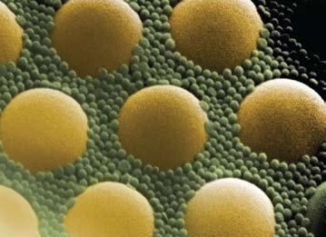
Vezenov has enlisted an ensemble of materials to overcome this shortcoming. He uses an organic linker to assemble a shell of cadmium-selenide nanoparticles (4 nm) and gold nanoparticles (20 nm) around a core formed by titania nanoparticles (20 to 40 nm).
“This is a porous catalyst with three networks,” says Vezenov. “The gold nanoparticles conduct electrons, while the titania nanoparticles do the electrochemistry to split water into hydrogen and oxygen. The CdSe nanoparticles, which are quantum dots, absorb the visible light.”
Sunlight plays a critical role in the reaction, Vezenov says, by exciting the titania electrons. As these electrons are “promoted” out of the filled valence band, they are replaced by electrons coaxed from the water, thus enabling the oxygen and hydrogen to split.
“We have generated some self-assembled catalyst films,” says Vezenov. “Because each of the materials linked has its own spectroscopic signature, we observed that they do indeed interact electronically after self-assembly. We are now checking for catalytic activity by looking for changes in the electrochemistry.”