
Duration: 14:08 | Published: July 12, 2023
Episode Summary
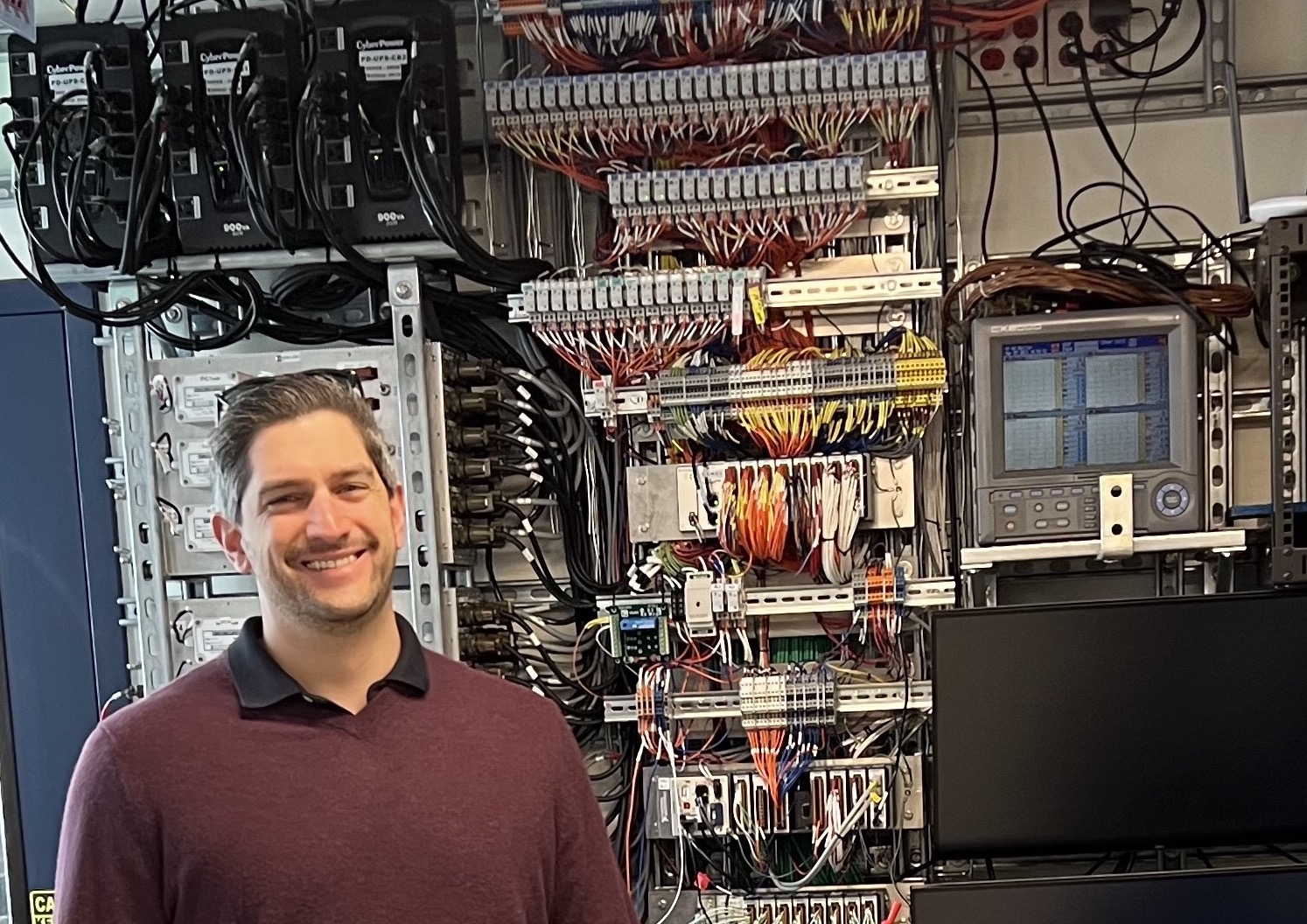
Cubic boron nitride is a super hard material with a lot of potential as a semiconductor to power modern electronics.
“Cubic boron nitride ends up being predicted to be even better than everything else we know today,” says Siddha Pimputkar, associate professor of materials science and engineering. “So I kind of joke it’s the holy grail material because the intrinsic properties are such that if we can grow this material and develop it into a device, it should outperform every other material system.”
In fact, the material has the potential to outperform silicon in speed, efficiency and durability. To date, however, no one has figured out how to grow the material in a scalable way. But Siddha and his team are developing a novel approach that could change that.
In this episode, Siddha explains the promise of cubic boron nitride, the historical roadblocks to growing it, and how advances in crystal growth could lead to more efficient power electronics, improved electric vehicles, stronger manufacturing tools, and more resilient energy infrastructure.
Key Moments
- 00:06 — Meet Siddha Pimputkar and the search for better semiconductor materials
- 01:30 — Childhood experiences that inspired a career in engineering
- 02:31 — Discovering materials science
- 03:02 — Why gallium nitride changed semiconductor research
- 04:30 — Looking beyond silicon to cubic boron nitride
- 05:35 — Why scientists call it the “Holy Grail” material
- 07:14 — Potential applications in electric vehicles and the power grid
- 08:57 — The challenge of growing large semiconductor crystals
- 09:52 — Developing a new approach to crystal growth
- 12:57 — Why solving difficult problems makes research worthwhile
Featured Quotes
"It gives me joy…to solve problems and make something." — Siddha Pimputkar
"It’s the Holy Grail material in the space." — Siddha Pimputkar
"What are you leaving behind for the next generation?" — Siddha Pimputkar
Full Transcript
Transcript is auto-generated and lightly edited for clarity.
Welcome to Rossin Connection, a podcast about all things Lehigh engineering. Coming to you from the P.C. Rossin College of Engineering and Applied Science at Lehigh University. It's a show for students, alumni, faculty and staff, current, former and future, and for anyone interested in the many creative ways that engineers are solving the world's problems. Today's episode features Siddha Pimputkar. He's an associate professor in the Department of Materials Science and Engineering. His trajectory as an engineer started like most people, as a kid, with no real idea what he wanted to do. Today he's developing a novel method of growing what he calls the Holy Grail of materials. One that could potentially be more powerful than silicon as a semiconductor, harder than diamond and capable of working in extreme environments. It's slow, uncertain work, but it fills him with purpose. Thanks for joining us. Siddha Pimputkar was born in the U.S. But he moved to Switzerland with his family when he was 10 and spent a lot of time in Germany with his grandparents. They'd built their own house and had a workshop in their basement and had gardens and a forest around their home.
So every summer when we would go, I would be spending six to eight weeks just building things, fixing things, cutting down trees,
And learning the skills you need to keep up a house.
Everything you know, needed maintenance like water, sewer lines, electricity, floors, tiling. We built out the entire attic of that house together so we know I did the insulation. I learned how to do drywall, learned how to put up walls, plumbing, electrical outlets and all that stuff.
He loved helping out learning how things worked, solving problems. So when it came time to start college and pick a major, he knew he was interested in engineering and science, but that's about it.
Yeah you know, to be perfectly honest, I had no clue what I wanted.
So he asked his dad
And his response was, well, mechanical engineering is great because it gives you a solid foundation in terms of logical thinking and having an ability to build and make things.
He went to college in Chicago for mechanical engineering and when he was a junior, started a minor in material science.
And that's really what struck my fancy then it was 'cause that's really a discipline that connects to all other engineering disciplines in some shape or form.
Siddha went on to get a PhD in material science at the University of California Santa Barbara, which is where he first started working with a material called gallium nitride. Gallium nitride is known as a wide bandgap semiconductor, which essentially means it can withstand higher voltages and operate at higher switching frequencies than traditional silicon semiconductors.
So gallium nitride at the time was relatively new, very exciting 'cause it has huge impact potential for optoelectronics and electronic devices. Um, but the material gallium nitride is actually a relatively challenging material to work with. And the reason it is challenging is because gallium nitride cannot melt under readily accessible conditions. And people have found ways around this, at least when growing thin films that are needed to make these LEDs or power electronic devices. But one of the things that definitely wasn't solved at the time and to even today hasn't really been solved is how do we grow very big single crystals of these materials?
Siddha spent his PhD and postdoc working on that problem, but to this day, researchers like him still haven't quite figured out how to grow these big crystals. In 2016, Siddha joined the faculty at Lehigh, and today he's focused on ultra wide bandgap semiconductors, materials that he says also have huge potential for making electronics super fast. He's looking at one material in particular, cubic boron nitride. And the problem? It's a familiar one, how to grow it, but like with gallium nitride, solving that problem would be a major breakthrough because the potential for cubic boron nitride as a semiconductor is huge.
So silicon-based technologies have an efficiency of low nineties percent on the conversion of electricity. So what that means is you're losing about 6% of the energy during this conversion process as heat. So you spent all this time and money to create this electricity and you're just wasting it 6% of it again. So that's kind of one of the driving forces. In terms of next generation semiconductors, it is enabling more efficient, more powerful devices than we can do today.
Another potential use is with radio frequency devices that emit waves to communicate like your cell phone.
And what we would like is more power higher frequencies. And silicon has a natural limitation in terms of how much power and how high of a frequency you can get. Whereas newer materials, the ones that we are working on, have this potential to leapfrog these material systems and outperform the existing ones by order of magnitudes. There
Are a range of alternatives to silicon being used today as semiconductors, but Siddha says cubic boron nitride could beat them all.
If you look at that landscape, cubic boron nitride ends up being predicted to be even better than everything else we know today. So I kind of joke it's the Holy Grail material in the space because the intrinsic properties are such that if we can grow this material and develop it into a device, it should outperform every other material system that we are currently aware of.
Those intrinsic properties include things like its thermal conductivity, which is the ability to extract and move heat through a device. Its ability to move electrons quickly through a material which is important for those radio frequency devices and its breakdown voltage.
And this is very important if we're making power electronic devices where if you think about grid scale applications, where we have kilovolt devices, we need a material that can withstand kilovolt potential differences across it and still be able to switch electrons.
Cubic boron nitride is also super hard, which makes it appealing as a manufacturing tool specifically for cutting iron diamond is actually a harder material thanks to its carbon composition, but it can't cut iron and that's because iron dissolves carbon.
So the diamond as a cutting tool actually slowly wears away, whereas cubic boron nitride from a chemical perspective is resistant to that action. So people would really like to make cutting tools based on cubic boron nitride to cut iron based tools and you can do so much more efficiently and faster, which kind of gives a leg up in the manufacturing spaces.
Siddha says one of the biggest impacts cubic boron nitride could make could be on power systems at the electric vehicle or grid scale,
You know, transmission lines across the United States. They have power stations where we down convert voltages and electricity gets kind of massive amounts of electricity funnel through these devices. So if we can switch to cubic boron nitride, we can certainly shrink them. We can make 'em more efficient, more powerful. We reduce the amount of waste electricity. I mean the potential impact is huge across many fields of kind of industry and research.
But that potential remains theoretical because to date, no one has figured out how to grow large single crystal nitrides in a cost-effective, scalable way. In part that's because growing cubic boron nitride requires extremely high temperatures and atmospheric pressure. For example, he says it takes tens of thousands of pounds of atmospheric pressure to form a diamond
Cubic boron nitride actually needs higher pressure than diamond to form, which typically leads to a lack of scalability, let's say industrially speaking to grow larger and larger volumes.
And what does industry want? Crystals big ones at least six inches in diameter. Ideally, he says up to 12 inches. Think of a crystal as a chunk of matter. Once grown that matter is cut into thin round wafers. Those wafers form the platform for making power electronic chips. The more chips you can get out of each crystal, the cheaper the electronics that use those chips. So size matters.
And that's where we need a new approach to grow cubic boron nitride under conditions that are not only lower pressure and more industrially scalable, but also a fundamental chemical pathway that allows for the scaling of that growth process to be continuous. And the evolution of a single millimeter scale crystal to grow into these 12 inch crystal chunks.
Siddha and his team are developing that new approach in part by using a precursor and a custom-built autoclave. And in case you've never seen one, an autoclave is essentially a tube with caps on either end at its most basic level. You can think of their approach like cooking meat in an Instapot. They'll heat up the system, turn the precursor into a liquid and initiate crystal growth in a way. They're really trailblazers with this research.
There's very few people in this world that actually have the equipment and the interest to grow and explore this space in general. So there's not too much information available to us in terms of how does the chemistry look like in these systems? Can we make predictions in terms of what works, what doesn't work? So we're doing a lot of foundational work in terms of exploring the space, working our way up to boron as a material system for crystal growth.
The goal for that growth?
A millimeter a day would be a phenomenal target. We don't really care if we just turn on an autoclave and walk away for three months. That's literally what industry does. They flick a switch, turn on their gas burners, come back three months later, take the huge crystals outta the autoclave and then cut them into the form that they wish. So knowledge that the process works is the most critical thing. 'cause if we know we can reliably grow at even 0.1 millimeters a day, economically speaking, like if you do the budgeting, it actually works out that you can sell a material at a price point that is affordable to industry and it actually makes sense to build upon as a platform. If we can scale the size of the autoclave, we can pack hundreds of crystals in those autoclaves at the same time. So even though it takes two to three months to do a single run, we're producing 200 crystals at once.
Those initial crystals that get put inside the autoclave that are essentially heated and squeezed until they transform into a potentially game changing material called cubic boron nitride, they're actually already tiny crystals of cubic boron nitride.
So the chicken and the egg problem kind of goes away for us because we already have the egg now we just need to grow the chicken. So someone else did a lot of hard work to get that egg. And that egg comes from a process called self nucleation where cubic boron nitride will spontaneously out of its own volition form under these very high pressure and temperature conditions. Okay, so it's like nature wants to be in the cubic boron nitride state at these very high pressures. So other folks have kind of created these environments where it just naturally starts to form and then grow to a a millimeter scale. And then the idea is we take those millimeter scale crystals, place them in our autoclaves and grow them to inch scale single crystals.
And in case you're wondering, because I was wondering, these starter crystals, if you will, are about the size of a rolled oat and you can get them in the mail for pretty cheap.
I was honestly a little surprised, but we bought this kilogram bag of it for a few dollars.
Like all fundamental research Siddha's work to create a scalable method to grow cubic boron nitride requires bottomless patients and no small amount of fortitude against the high probabilities of failure. But the potential is always right there, and that's what drives him.
It gives me joy, pleasure to kind of solve problems and make something. So I think kind of having that I have something in my hands that I made, no one else can. You know it's a certain thing of what's the purpose of your life? What are you leaving behind for the next generation for society that improves this world?
That's it for today's show. I'd like to thank Siddha for taking the time to share his research. For more information about all the academic programs at the P.C. Rossin College of Engineering and Applied Science, and to find our show, head to engineering.lehigh.edu. Music in this episode is by Blue Dot Sessions. You can send us story suggestions or feedback on X at Rossin podcast. I'm your host and producer, Christine Fennessy. See you next time.
About the Guest
Siddha Pimputkar is an associate professor in Lehigh University’s Department of Materials Science and Engineering. His research focuses on crystal growth, wide-bandgap and ultra-wide-bandgap semiconductor materials, and advanced manufacturing techniques for next-generation electronics. His laboratory is developing scalable methods to grow cubic boron nitride crystals for applications in power electronics, communications, manufacturing and energy systems.
Episode Details
Related Episodes
- Episode 22: The "Magic" Behind the Materials That Power Modern Technology
- Episode 27: Powering a More Reliable Electric Grid with Javad Khazaei
- Episode 29: Making Medicines Easier to Deliver with Whitney Blocher McTigue