Researchers in Lehigh’s Center for Optical Technologies (COT) have received three NSF grants and one DARPA award for wide bandgap semiconductor research that could lead to highquality, energy-efficient lighting systems as well as lightweight bioterrorism-prevention devices.
The group hopes to reduce the number of defects that occur during fabrication of compound semiconductors, usually in the crystalline structure. Its members are conducting nanoscale experiments into semiconductor substrates, and they are exploring a new field called “spintronics,” in which light signals are employed to manipulate the spin, or orientation, of the electrons of magnetic materials.
The researchers are particularly interested in indiumgallium-nitride semiconductors, which are used to make blue light-emitting diodes (LEDs) and lasers, and in aluminum-gallium-nitride semiconductors, which are used to make ultraviolet LEDs and lasers.
The wide bandgap semiconductor group includes Prof. Volkmar Dierolf of physics; Profs. Helen Chan, Richard Vinci and Slade Cargill of materials science and engineering; and Profs. Nelson Tansu and James Hwang of electrical and computer engineering.
The researchers take a multifaceted approach to defects, which undermine a material’s semiconductor properties and cause faulty devices. Their goal is to reduce the number of defects and confine them to non-light-producing regions of the semiconductor.
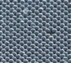
Vinci and Chan are attempting to alter the surface of sapphire wafers, commonly used as substrates for semiconductor and laser materials, with nanostructures, thus enabling light-emitting materials to be grown directly on the surface. This will allow Tansu to grow high-quality semiconductors using a process called nanoheteroepitaxy.
Tansu is seeking to improve the nanoscale light-producing capacity of the semiconductor materials for LEDs and lasers.
“We are using quantum mechanics to engineer the atomic arrangement in the nanoscale active regions, such that the rate of light generation is significantly improved,” says Tansu. “This can be done by optimizing the arrangement, composition, thickness and other parameters of the fewer than one dozen atomic layers of semiconductor films that make up a nanoscale active region.”
Dierolf, leader of the wide bandgap team, is characterizing the optical properties of the semiconductor and laser materials at the nano-region. He is also investigating the possibility of making gallium-nitride a ferromagnetic material by doping the compound with ions from rare earth elements.
These efforts are leading him into the field of spintronics, in which scientists and engineers, working at the nanoscale, use an electron’s spin rather than its full charge to create electronic devices.

