|
“This system will give Lehigh a unique capability in materials characterization research.” |
Lehigh researchers are transforming an aberration-corrected scanning transmission electron microscope (STEM) into the equivalent of a synchrotron facility (a football-field-size particle accelerator), with greatly improved spatial resolution and versatility.
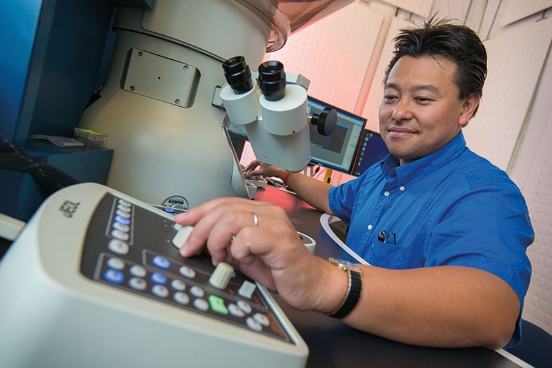
This upgraded instrumentation system, which integrates an electron energy loss spectrometer (EELS) into the aberration-corrected STEM (a 3-meter-tall instrument housed in Whitaker Lab) would expand scientists’ ability to characterize the chemical composition and bonding status of elements within a material down to the single-atom level, says Masashi Watanabe, an associate professor of materials science and engineering.
In electron energy loss spectrometry, a thin sample of a material is hit with the powerful electron beam of an electron microscope. The EELS measures the changes in kinetic energy of electrons as they interact with the sample, which allows scientists to determine the elemental composition and to interpret chemical bonding status of materials. The technique is an alternative to synchrotron-based x-ray absorption spectrometry, but current implementations at large-scale facilities can’t offer information at the nanoscale.
“Even at the national labs’ powerful synchrotron facilities, there is no instrument that can get this high spatial-resolution information, this level of detail at the nanoscale, that we’re targeting,” says Watanabe. “With a successful prototype that meets our goal of increasing spatial resolution by 1000 times over current integrations, we see important applications in areas like semiconductors, advanced alloys, and catalysis—and the potential for an overall paradigm shift.”
It’s an advance that could usher in a new era in materials characterization.
The team is partnering with Japanese electron microscope manufacturer JEOL and German electron optics company CEOS to create the prototype. It will include an EELS spectrometer with improved optics design for the detection of higher energy-loss electrons and an ultra-high-sensitivity electron detector for limited signal detection in the high-energy-loss range. Current EELS spectrometers cannot detect energy-loss electrons higher than 3,000 eV; the new system will have capabilities up to ~13,000 eV.
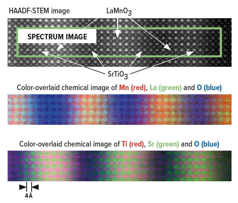
The system will include a multifunctional scan generator for flexible electron probe control. The Lehigh team will also develop an integrated software platform to efficiently control data acquisition while maintaining high spatial resolution and allowing energy-filtered imaging. Watanabe expects to gather elemental distributions at the atomic scale (as shown in the example of electron energy-loss images from a complex oxide multilayer sample) once the system development is completed.
 This instrument controlling scheme has been developed through the Presidential Nano/Human Interface Initiative led by Martin Harmer, Alcoa Foundation Professor of Materials Science and Engineering.
The project was awarded a three-year, $625,000 grant from the NSF’s Major Research Instrumentation Program. Watanabe, who is one of the organizers of the Lehigh Microscopy School, is leading the system’s development. Fellow faculty members Helen Chan, Himanshu Jain, John DuPont, and Christopher Kiely are co-PIs on the project and will test the instrumentation in their various research areas. The proposal was coordinated through Lehigh’s Institute for Functional Materials and Devices (I-FMD).
“We’ll be able to expand the materials we can investigate through EELS analysis to include, for example, gold nanoparticles in catalytic applications, high-entropy alloys with heavy elements, and rare-earth-based LEDs,” Watanabe says. “It will give Lehigh a unique capability in materials characterization research.”
CREDIT: Images produced using EELS, like this example, help scientists better understand elemental distributions within materials at the atomic scale and interpret their chemical bonding status. Results obtained in collaboration with JEOL.